MSc thesis project proposal
Flip-chip interconnect by use of in-substrate embedded heaters
Project outside the university
CITCThe continuous increase in data consumption is driving the technology requirements for packaging of integrated photonics chips. Future application requirements such as increased bandwidth (for e.g faster internet) and increased density of optical and electrical functions per chip area will require ultra-high density flip-chip interconnect.
However, the state of art in current photonic system assembly is electrical interconnect by wire bonding, optical interconnect by active alignment, and bonding of fiber assembly unit in front of the die - a technology that is not compatible with future requirements.
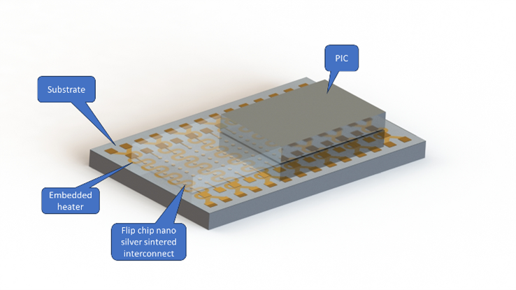
A solution may be found in nano-metallic sinter technologies, which can potentially enable a process scheme for packaging integrated photonic dies with both electrical and optical interconnects in one process. Such a process will not only increase the performance of the device, but also provide benefits for the assembly of the product. This assembly process requires innovative assembly technologies, which enable active alignment in a flip-chip configuration. Since nanopaste sintering requires local heat pulses, the idea is to add heaters in the assembly fan-out substrate to locally introduce heat for nano sintering the flip chip interconnect during or after active optical alignment.
Using cleanroom fabrication technologies such as thin film deposition, lithography and etching, a fan-out substrate with embedded heaters will be fabricated. State-of-the-art assembly, packaging and active alignment equipment is used to demonstrate the feasibility of the flip chip interconnect technology.
Assignment
This project will be developed as a collaboration between TU Delft and CITC. It will focus on the fabrication of an interposer with embedded heater structures, study nano sinter flip chip technology, and demonstrate this technology in combination with active optical alignment.
Project activities
- literature study to assess the state of the art
- Design of fan-out substrate with embedded heaters
- Flowchart design for processing in the EKL cleanroom (TU Delft)
- Study nano sinter flip-chip interconnect technology (CITC assembly lab)
- Demonstrate process in combination with active optical alignment (CITC assembly lab)
- Cleanroom process training (TU Delft)
- Back-end assembly training at CITC
- Fabrication and device/assembly characterization
- Reporting
Daily supervisor: Dr. Henk van Zeijl
Requirements
You are an ambitious master student looking for a challenging thesis project on a microelectronics packaging problem. You have a physics, material science or microelectronics background and an interest in microfabrication technology. Good communication skills in English and a pro-active attitude are expected.
Contact
prof.dr. GuoQi Zhang
Electronic Components, Technology and Materials Group
Department of Microelectronics
Last modified: 2024-03-15